
If you have
decided to move or remove a track or component, the Undo function lets you
cancel this decision and return to the previous situation. Redo is used to
cancel an Undo. Using these options you can experiment with your design to your
heart�s content while still being able to return to previous situations.
Layo1 PCB
for Windows offers an arsenal of layers. You can use up to 16 layers for copper.
In addition, documentation layers for silkscreen, soldering mask, soldering
paste, assembly etc. are available.
Layo1 PCB
for Windows does not limit you to 9 zoom options. As well as Zoom-In and
Zoom-Out you can use Zoom-All and Zoom-Window.
Layo1 PCB
for Windows has a new database format for PCB designs. This database contains the entire PCB design including:
Layo1 PCB
has an internal resolution of 0.0001mm. This enables you to design PCBs with
very high resolution.
Database
items are displayed and can be modified in tables. This enables a clear overview
of, for example, the Netlist, layers and padstacks.
Layo1 PCB
for Windows enables you to define the shape and dimensions of a Pad/Via per
layer. A padstack gives the full picture of a Pad/Via including the drilling
diameter.
These
templates are comparable to those used in Microsoft Word. A template is
therefore a basic PCB design with settings for the number of layers, grids,
colours, post-processing, pads, etc. The dimensions of the PCB design are also
in the template. You can even make templates with components (i.e. connectors)
and fixing holes. Templates can save you a lot of time and hard work. Of course,
you can design your own templates. If you wish, you can convert a PCB design
into a template.
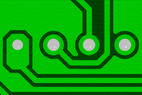 |
| Dead copper is not generated.
|
 |
| You can also enter a cartridge under every corner! |
The
Auto-Backup option allows you to automatically backup your PCB design. You can
set the time interval between backups and the maximum number of backups. You can
also designate where to save backups.
In contrast
to Layo1 PCB for DOS, the Online Design Rule Checker in Layo1 PCB for Windows
will alert you of any error immediately (i.e. not once the error has already
been made). Of course, you can also execute a DRC-All at any time. The DRC does
not only test for copper but also for drilling holes. This prevents you from
placing a track where there is a drilling hole, for example.
Generating
Post-Process data (Gerber/Excellon) is a lot easier. A couple of key hits are
sufficient to generate the Gerber and Excellon files. The settings you create
are stored in the PCB design. For instance, if you wish to generate Post-Process
data for a Re-Design, you do not need to go through all the settings all over
again. Post-Process settings can also be set in templates.
Most PCB Factories prefer Extended Gerber (274-X). The definitions for all the Apertures required are already in the Gerber files.
Information
for component setting machines (Pick and Place) can be stored in a text file.
You can of
course effortlessly change over from your Layo1 PCB for DOS version to Layo1 PCB
for Windows. You can import all your designs and the component library and use
or modify them. Your investment is safeguarded with Layo1 PCB for Windows. The
conversion is transparent and does not require any excessive effort from you.